Products & solutions
Products & solutions
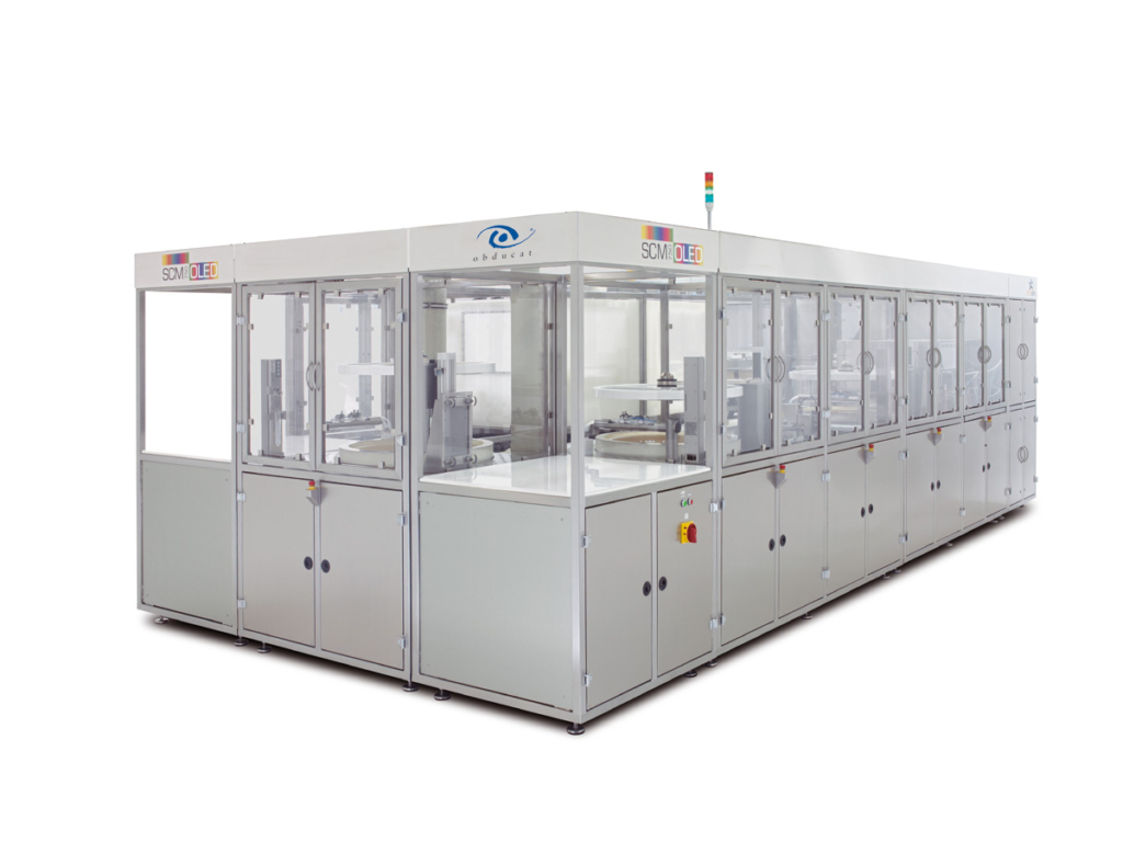
MCT Large Substrates
FULLY AUTOMATIC MICRO-CLUSTER TRACK (MCT) TOOL FOR COATING & DEVELOPING
Obducats MCT Large Substrate system provide excellent performance as a result of the embedded cutting-edge solutions derived from many years close cooperation with our customers.
This ensures that the system is prepared for current and future high-volume manufacturing (HVM) requirements at a competitive Cost-of-Ownership. The configuration flexibility of the MCT Large Substrates makes it adaptable to processing requirements in a wide variety of applications such as Optics, Displays and Advanced Packaging.
Highlights
Suitable for High Volume Manufacturing (HVM)
High reliability, yield and uptime
Highly configurable tool
Customization possible for specific customer process and throughput reuirements
Substrate size
| System | Substrate ⌀ | Square substrates |
|---|---|---|
| MCT 600 | 600 mm | 450 mm * 450 mm |
| MCT 775 | 760 mm | 540 mm * 540 mm |
| MCT 1200 | 1000 mm | 850 mm * 850 mm |
| MCT 1500 | 1400 mm | 1000 mm * 1000 mm |
Tool Configurations
The standard MCT Large Substrates configuration is equipped with an I/O station and an multi axis robot system on a linear track. It can incorporate up to 10 modules configured for Coating, Developing and/or Thermal processing.
Coating is performed using the standard open process bowl and a standard vacuum chuck. This ensures a uniform and repeatable coating process. As an option the open bowl module can be replaced with our Rotating Covered Chuck Technology (RCCT™) module. (See tool options)
The developer can perform both puddle and spray-based processes.
The Thermal processing units can be equipped with up to 8 temperature plates in a stacker – hot plates, cool plates & HMDS vapor prime hot plate. The hot plates have a programmable temperature range up to 300°C and are equipped with programmable proximity pins.
The HMDS vapor prime hot plate has a programmable temperature range up to 200°C. The process is fully automated and adheres to all recognized safety standards.
Easy to operate windows-based PC with 22” color touch screen
Unlimited process recipe / flow storage capacity plus USB port
Batch & process parameter tracking
Ethernet port
Tool Options
Coater Module – Rotating Covered Chuck Technology (RCCT™)
Obducat’s revolutionary Rotating Covered Chuck Technology (RCCT™) process environment design provides for:
Completely sealed solvent saturated atmosphere
Minimal turbulence around the substrate eliminating rotational corner effects on squared substrates, enabling industry leading resist uniformity across the entire substrate at lower spin speeds.
Superior coating uniformity on submicron layers as well as for thick resist layers compared to open bowl.
Reduced process cost and improved environmental profile by lowering material consumption.
Eliminating the need for Backside Rinse (BSR).
Edge Bead Removal (EBR)
Obducat’s high performing EBR technology is used to remove the build-up of material at the substrate edges after spin coating. Removal of the edge bead prevents stepper focusing problems and any build-up of photoresist on the backside of the wafer. It also prevents ‘chipping’ of the photoresist that could cause contamination issues.
Obducat offers three types of EBR processes – standard solvent based, SmartEBR by either solvent based process or UV exposure process.
The standard solvent based EBR process uses a programmable nozzle directing the solvent fluid towards the substrate edge thereby removing the edge bead during spinning.
For SmartEBR solvent based process the exact shape of a square substrate is first determined by a sensor. Knowing the geometry of the substrate, the system can remove the edge bead by moving the substrate while applying solvent from a programmable nozzle.
For SmartEBR UV exposed based process, the exact substrate shape is similarly determined but in the following step the edge bead is exposed to UV light. This UV exposure allows for the edge bead to be removed in a later process step.
Multiple Chuck solutions – Vacuum, Low contact
Chuck solutions for coating:
In case the backside has active areas, the use of an edge handling chuck with an edge exclusion of typically 4mm is recommended.
Glass substrates are very sensitive to temperature gradients. Since vacuum substrate handling may cause such temperature gradients, Obducat offers glass substrate handling by corner suction cups with alignment pins minimizing these gradients.
Chuck solutions for developing:
For round substrates that are wet treated the low contact chucks are used, where the substate is held in place by supporting pins and centripetal force fixing it during the high-speed drying.
Squared substrates are held at the corners by alignment pins using low contact chucks. The advantage of this chuck is the entire backside can be rinsed.
Environmental Control Unit (ECU) and Filter Fan Units (FFU)
To guarantee superior process stability and high yields, the tool can be equipped with an ECU, this will control the temperature and humidity in the processing area. FFU’s can be connected to the ECU to ensure a particle free environment.
Temperature controlled resist and chemical lines
Photoresist
A key process parameter for coating uniformity is temperature control. To enable a high level of coating uniformity, the tool can be equipped with temperature-controlled photoresist lines that will enable a repeatable temperature level of the photoresist substrate-to-substrate at point of dispense.
Developer chemicals
When chemicals are supplied from the fab supply or stored outside the cleanroom the temperatures are different to the cleanroom environment causing chemicals to react and perform differently with changes in temperature. This can result in processing variations. This option can ensure a repeatable temperature level of the chemical’s substrate-to-substrate at point of dispense.
In-line film thickness measurement
The high performing measurement method uses white light interferometry, where a low pass filter blocks all wavelengths below 450 nm to protect photoresist from being exposed.
In-situ film thickness measurement in real-time enables immediate quality control and yield monitoring.
High speed wafer mapping with a programmable x-y stage can provide relevant data input towards root cause analysis of coating failures.
Connection to wafer fab Management Systems
The tool can be configured to enable connection to various Manufacturing Execution System (MES) interfaces such as:
SECS/GEM
OPC/UA
Customer specific interfaces