Products & solutions
Products & solutions
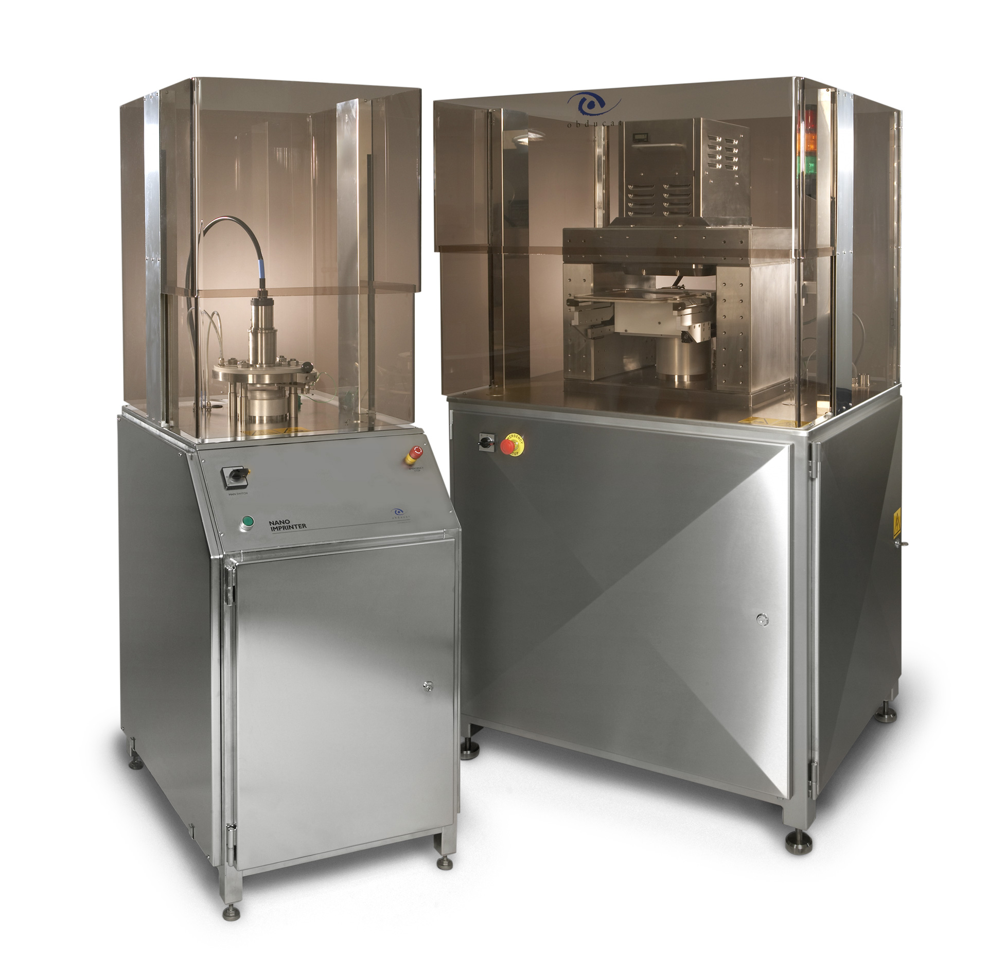
SINDRE® Integra
NIL TOOLS FOR HVM
A fully automated nanoimprint lithography tool suitable for high-volume manufacturing within several application areas with throughput of up to 70 WPH. Allows for imprint size up to 12” wafers. Because of its high repeatability, low maintenance cost and high yield the SINDRE® Integra tool provides a competitive Cost-of-Ownership.
Highlights
Fully automated production tool
Industry leading Cost-of-Ownership
Up to 70 wafers/hour and high yield
In-line CVD anti-stick of IPS®
In-line IPS® resist coating
Sub 50nm resolution
Key Features
- The fully automated SINDRE® Integra NIL tools provides reliable, high volume manufacturing capabilties – combining sub 50 nm resolution and excellent CD-control.
- The SINDRE® Integra tools enables cost-efficient high-volume manufacturing. High quality engineering ensures high repeatability, low maintenance cost and a high yield – all this provides for a highly competitive CoO.
- The SINDRE® tools are suitable for use within several application areas such as Optics and Photonics, Bio and Medical Devices, LEDs and Micro- and Mini LED displays, MEMS and Sensors.
- The SoftPress® technology ensures imprint uniformity all the way to the edges of the substrate, without the need of any planarization layers.
- IPS® technology increase stamp life and eliminates the risk of substrate breakage. The manufacturing of the IPS is integrated into the system which ensures high quality contamination free working stamps.
- In-line IPS® resist coating.
- Configurable UV-intensity levels from 100-400 mW/cm2 at substrate levelThe tools repeatable performance enables a simple up- and downstream processing.
- In-line CVD anti-stick of IPS enabling higher yield and reducing material compatibility issues enabling a wider process window.
- Customized configurations for different substrate sizes and shapes possible.
- Designed according to European safety regulations and CE Mark.
Obducat’s NIL Process Technologies

IPS® – Intermediate Polymer Stamp
The patented IPS® technology is based on making a replication of the master stamp into a soft Intermediate Polymer Stamp (IPS®). The IPS ® is then used in a second imprint step to transfer the structures onto the target substrate. The IPS® enables contamination control, increases the master stamp lifetime and makes the imprint process less sensitive to substrate contaminations and surface roughness.

SoftPress®
With Obducat’s patented SoftPress® technology, the imprint pressure is applied using compressed gas, ensuring pressure uniformity over the entire imprint area. This allows the stamp or IPS® to conform to the substrate, eliminating negative effects from thickness variations, bow or waviness. SoftPress® enables thin and uniform residual layer across the substrate, which is critical for enabling high-resolution imprinting and pattern transfer fidelity.

STU® Simultaneous Thermal and UV
The patented STU® technology combines, in one imprint sequence, the simultaneous use of thermal- and UV based imprint processes. The STU® process allows for increased polymer flow rate giving a shorter process time as well as enabling improved material compatibility and thereby a wider selection of workable imprint materials.

Automated IPS® application and demolding
The patented automated demolding function developed by Obducat for use with the patented IPS® and SoftPress® technologies makes the application of the IPS® material accurate and repeatable, ensuring that the pattern fidelity is maintained. The automated demolding function also protects the stamp from any manual handling during the imprint process.

In-line IPS® resist coating
The in-line resist coating of the IPS®, allows for a much wider selection of carrier film material as well as IPS resist material. The customer will have the possibility to tailor the process by matching carrier materials and resist materials. Furthermore, the customer can also optimize the selection of the IPS materials to maximize the number of times the IPS can be used.